People in the development of new products, often eager to realize the function of the product, then use low frequency and low speed experience, satisfied with using the software to connect single chip, chip and components, they hope to achieve product function, performance and performance, instead, not only is at a low level, but also delayed the precious time.
In fact, with the integrated circuit clock rate increase, rise and fall rate, reduced supply voltage and continuously improve and shorten the product complexity and intensity of the design cycle, with low frequency, low-speed experience has been completely unable to achieve product function, performance and performance. If re design in the later stages of product design, then the cost is high, if the delay date, the loss is even greater
Therefore, the design goal to launch the first product ", is the need for a life-and-death matter competition. In the first time to achieve product requirements, make product performance to give full play, and to achieve maximum performance, we must do a good job in EMC design. In order to solve the EMC problem with the lowest cost, it is necessary to design the EMC in the function design, and select the correct method
Now, the focus of product design has shifted from functional design and logic design to EMC design
EMC design should be the correct method: tackling the problem, focusing on a cure. Is from the management of the electromagnetic compatibility of the source of the problem, according to the importance of successively, divided into several levels of design, and make a comprehensive analysis and make appropriate adjustments, until perfect:
The first layer is one of the main problems: the selection of active devices and the design of printed circuit board
The second layer is focused on the fundamental problem of the two: grounding design
The third layer is one of the following: structural / shielding design
The fourth layer for the treatment of the two: filter design
The fifth layer is the treatment of the following three: Transient Disturbance Suppression Design
The sixth layer is system level EMC design
At the same time, the integrated design of grounding, shielding and filtering, and the software anti disturbance design. This is called the "electromagnetic compatibility layered and integrated design method", which can be used as a successful test of electromagnetic compatibility
Electromagnetic compatibility and integrated design method is the author of the May 2000 "national electromagnetic compatibility standards and Quality Certification Seminar", the first proposed, has been more than ten years. In the country more than ten years, a number of enterprises have out "test method" to modify the electromagnetic compatibility test failure of the "vicious circle", so in the beginning of the product design, on the initiative of EMC design. Moreover, EMC design input only 1% (domestic is generally 5% to 10%). Cost is reduced, and shorten the time. At the same time, the electromagnetic compatibility layer and integrated design method is more substantial and perfect, many enterprises and units received national recognition.
The selection of the first active device and the design of printed circuit board
In the source of electromagnetic compatibility problems, the fundamental solution to the EMC problem, we must first do a good job in the selection of chips and printed circuit board design.
Sensitivity and emission characteristics of active devices
1 electromagnetic sensitivity characteristic
The sensitivity of the device is dependent on the sensitivity and bandwidth, and the out of band sensitivity is characterized by out of band rejection
The sensitivity of the logic device depends on the noise tolerance or the noise immunity, and the out - of - band sensitivity is also indicated by out - band rejection.
2 electromagnetic emission characteristics
Logic device is one of the most common broadband disturbance sources, and the shorter the rise time of the clock waveform, the wider the bandwidth of the corresponding tr
BW=1/ptr
This bandwidth is also the highest frequency component. The actual radiation frequency range may reach ten times more than BW. The typical value of TR can be found through the device manual.
It is generally believed that: in the PCB design, need to consider the problem of clock frequency, in fact, the rise time of the TR clock waveform is the most critical factor. The rise time is defined as tr increased from 10% to 90% at the waveform of time. If the premises need to input at one end of the interconnect requirements of Fang Bo, at the other end have a square wave, the interconnect must not only can transfer the fundamental wave, also must be able to transmit all harmonics, at least 15 harmonics. That is to say, the clock frequency of PCB is not important, to produce harmonic tr rise time and needs is the most important. This is the word to describe the bandwidth of BW. That is the highest frequency component.
Harm 3 Delta I noise current, transient load current IL
When the digital integrated circuit in the power supply work, it will be the internal door circuit will be "0" and "1", that is, the switch state. In the process of transformation, the transistor gate circuit in the conversion will occur and the off state conduction, there will be transient current - inrush current from the power flow di/dt entry circuit, or into the ground from the gate, the source of this change is the initial current Delta I noise, called Delta I noise current. As shown in figure 1.
Figure 1 I noise current
The capacitance of the driving line to the ground and the input capacitance of the driving door are the load capacitance Cs, which is normally charged, and the value is the power supply voltage. The driving gate is switched from high potential to low Cs, and the discharge current is called transient load current:
IL = Cs * dv/dt
The transient load current of IL and delta I noise current composite, EMI will produce stronger. Is the product function, which hinder the realization of provisions of main reasons of product performance can not be brought into full play. Because of PCB, signal line, power line and ground wire are lead inductance L. The transient load transient current di/dt current IL and delta I noise current generated by the composite, inductance lead inductance L due to the peak voltage
Ldi/dt - V=
The delta I noise voltage, called simultaneous switching noise (Simultaneous Switch Noise SSN), as shown in Figure 2, will lead to potential and power supply voltage fluctuation (Ground/Power, Bounce) generated EMI. Therefore, L is one of the causes of lead inductance conduction and radiation harassment harassment.
.jpg)
Figure 2 peak voltage
Another source. The source impedance of EMI for equivalent voltage source, the input impedance of the Z power distribution system, system requirements. The peak voltage should be within the normal power supply voltage of + 2.5% to + 5%. Equivalent to the source impedance Z to be low enough.
V= Z * I
No matter how to change a I, which can keep the V change is very small. This can be reached through the installation of decoupling capacitor.
The source impedance of the ideal power supply Z is zero, and the potential at any point on the power plane remains constant
4 master IC design and packaging features to inhibit EMI
IC packaging is also one of the causes of electromagnetic interference. The IC package includes the chip, the internal PCB and the pad, which directly affect the capacitance and inductance of the IC package
As a part of the system, the silicon chip has to be packaged in a package and then soldered to the PCB board. The interconnection chain, which is connected to the PCB board through a package, is a complex system in itself.
The chip design, packaging, and printed circuit board should be considered as a system to ensure that the final assembly and power supply can achieve the desired results. The best approach is to design, analyze, and validate all of these.
Package refers to the installation of a semiconductor integrated circuit chip with the shell, it not only plays placed, fixed, sealing, protection and enhance the performance of the electric heating chip, chip and Bridge - contact or communication with the outside world circuit chip on the outer shell with a wire connected to the package pins, the pins and printed by wire in the connection with other devices. The establishment of an important indicator to measure the chip package technology is advanced or not is a chip area and packaging area ratio, the ratio is close to 1 as possible, lead inductance is small. Packaging technology has gone through several generations of change:
1) through hole encapsulation (Through-hole Package)
DIP (Dual In-line Package) dual in-line package: in 70s the last century of the package, the maximum pin number 64. The area of the chip / package area is 1:8.6, far from 1, indicating the encapsulation efficiency is very low, long fuse, large lead inductance;
PGA (Pin Grid Array) pin grid array package, pin center distance of 2.54mm, the number of pins for the 64-447. surface mount PGA pin center distance of 1.27mm, the number of pins is 250-528, lead inductance is very large;
2) surface mount package (Surface Mounted Package)
In 80s the chip carrier package, ceramic leadless chip carrier package LCCC, plastic leaded chip carrier package PLCC, small package size SOP (Small Outline Package), plastic quad flat package PQFP. chip package area / area 1:7.8, inductance is still great;
3) BGA package and CSP package
In 90s with the use of integrated technology, and the deep submicron technology LSI, VLSI, ULSI have emerged, chip integration continues to improve, more strictly to the packaging requirements of I/O pincount increased sharply, power consumption increases. To meet the needs of the development, based on the original packaging varieties, and add variety - the new ball grid array package BGA (Ball Grid Array Package). A high density, CPU north and South Bridge such as VLSI chip with high performance, the best choice of multiple function and high I/O pin package. The area of the chip / package area is 1:4, the lead inductance decreases; in September 1994 was born in the name of a new package the chip scale package (Chip CSP, Size Package or ChipScale Package), chip area / package area is 1:1.1., that is to say, how big is the single chip, the package size is as big, lead inductance is greatly reduced;.
4) bare chip assembly
With the increasing of the density of assembly and the integration of IC, in order to adapt to this trend, the bare chip assembly of IC comes into being and has been widely used. It is cut from the finished wafer (Water) on the chip, not in accordance with the traditional IC packaging in advance, and the chip directly assembled on the circuit board, which is called Bare Chip Assembly. Early COB (Chip on Board) is the specific use of bare chip, but COB is the back paste chip on the board, and then lead rubber seal. And a new generation of Bare Chip and even lead to the chip is also saved, the positive electric pole, directly welded on the surface of each buckle with point (Flip Chip). The utility model is characterized in that the lug of the chip is buckled and connected on the inner foot of the automatic bonding (TAB) of the carrier tape, and is connected with the PCB on the outer pin. These two new assembly methods are known as bare chip assembly, parasitic C, L small, and can save about 30% of the overall cost;
5) tape automatic bonding (TAB): multi pin large chip assembly: one of the bare chip mounting technology
Carrying the material for the polyimide film covered on the surface of copper foil after corrosion, a fine wiring pattern by chemical method. The chip is plated with Au, Cu or Sn/Pn alloy on the extraction point to form a bump electrode with a height of 20-30mm. The assembly method is that the chip is pasted on the carrier belt, and the bump electrode is connected with the lead wire of the carrier tape. It is suitable for mass production automation. TAB lead spacing can be further reduced to 0.2mm or less than QFP.
(6) system chip (SoC)
SoC is all functional modules are integrated into a single chip system. A SoC compared with the current board, which may contain the function modules are: CPU, RAM, ROM, DSP, wireless module, analog and digital module, network module, core etc..
The embedded system integrates the whole embedded system into a chip, and the circuit board of the application system is concise, the volume and the power consumption are reduced, and the reliability is improved. Moreover, by changing the internal working voltage, reduce the power consumption of the chip chip; reduce external pin count, simplify the manufacturing process; to reduce the external signal between the driving unit and the interface circuit board transfer, speed up data processing; embedded circuit can avoid the external circuit board in the signal transmission caused by the harassment.
Single chip Unit microcontroller (MicroController, MCU), commonly known as single-chip microcomputer, the entire embedded microcomputer system integrated into a chip, so that power consumption and cost reduction, increased reliability.
The development of IC technology industry experienced IC integration, function integration, technology, until today, based on the knowledge of computer hardware and software integration, and its goal is the electronic product system circuit continuously integrated into the chip, to devour the whole product system. The emergence of a single chip embedded system, a single chip to achieve the product system is not limited to the hardware system, but with a flexible performance of the hardware and software collection of electronic systems. SoC is the ultimate goal of microelectronics IC design
Two. Printed circuit board design
With the development of information technology, the speed of transmission and processing of signals is getting faster and faster. It has become one of the most important problems in PCB design. PCB is not only a platform for supporting electronic components, simply on the base metal wire, because of the existence of lead inductance, and can not achieve interconnection. PCB has become a functional component to become a high-performance system architecture. So that the design of PCB becomes the key factor to the success of product design.
Printed circuit board EMC design is the basis for the design of the product EMC. The radiation emission of the whole machine is over standard, and the radiation sensitivity is not up to standard, which is caused by PCB.
In the PCB design stage to deal with the EMC problem, is the most effective means of achieving electromagnetic compatibility, the lowest cost means
1 one of the methods to suppress electromagnetic interference emission: the basic principles of PCB routing and layout
The current must flow in a loop. Each signal has a loop to form a loop. DC and low frequency, the loop current is always the least resistance from the path through; and high frequency, the return is always from the impedance of the smallest path through.
The current flowing through the signal wires are respectively equal in opposite directions and the return current, the magnetic field is equal to the size of their direction on the contrary, if the two wires are very close, namely the magnetic field differential mode EMI radiation will be fully offset. So the basic principle is: if we want to reduce the differential mode EMI radiation to the minimum, the signal line should be as close as possible to the loop line with it, that is, the loop area must be reduced to a minimum.
Careful design can reduce the disturbance caused by the line impedance to a great extent, and suppress the electromagnetic interference. When the frequency is more than kHz, the impedance of the conductor is mainly determined by the inductance of the wire, the thin and long loop wire presents a high inductance (typically lOnH/cm), and the impedance increases with the increase of the frequency. If the design is not handled properly, the common impedance coupling.
Two parallel wires current in the opposite direction, due to mutual effect, can effectively reduce the inductance, the total inductance can be expressed as:
L = +L2 2M - L1
In the formula, L1 and L2 are respectively 1 and 2 of the lead wire inductance, mutual inductance M
M=L1/[1+ (a/h) 2]
Formula, a- distance, h- distance from ground. When: L1 = L2, then:
=2 L (M L1-)
When: a = 0
M = L1
, then L = 0
The basic principle of the wiring can be obtained. For example, the distance between the multilayer board layer is very small, the 4 plate is 0.15mm, and the 28 layer 0.05mm can really do loop area is zero, the total inductance is zero, as shown in figure 3.
Figure 3 wiring basic principles: loop area is zero
.jpg)
In the layout of the printed circuit board, we should first carry out the physical partition and the electrical partition, determine the position of the components on the board, and then arrange the ground wire, power line, and then arrange the high-speed signal line, and finally consider the low speed signal line.
Layout, the first to make a good compatibility, the location of the components should be based on the supply voltage, digital and analog circuits, speed, current size and so on, so as not to interfere with each other. According to the position of the components, the arrangement of the pins of the printed board connector can be determined. All connectors shall be arranged on one side of the printed circuit board, as far as possible from both sides of the cable, to reduce common mode radiation. Secondly, it should meet the requirements of installation, force, heat and beauty
(1) power cord
Under the condition of safety, the power supply line should be as close as possible to the ground wire, so as to reduce the area of the differential mode radiation and to reduce the interference of the circuit. For a single power supply PCB, a power plane is enough; for a variety of power, if not mutually staggered, can be taken as a reference power supply layer segmentation, surface, and sewing for the power capacitor; each other (especially a variety of power supply, and staggered IC) single board, must be considered by 2 or more power plane.
(2) the position of the clock line, signal line and ground wire
The distance between the clock line and the signal line is close to the surface of the ground or the distance between the earth and the earth. If necessary, both sides of the ground wire escort.
(3) according to the logical speed
When you need to quickly layout, medium speed and low speed logic circuit on the circuit board, high-speed devices (fast logic, clock oscillator) should be placed in close proximity to the edge connector range, and low speed logic and memory, should be placed away from the connector range. This is beneficial to the reduction of common impedance coupling, radiation and interference.
(4) to avoid the discontinuity of the printed circuit board wire impedance characteristics, ensure the characteristic impedance must be continuous, trace width mutation, do not suddenly don‘t lead the corner, the width of the wiring layer must be continuous, different layers of wire impedance must also be continuous.
(5) check whether the signal line length and frequency of the signal of resonance, i.e. when the wiring length is integer times when the signal wavelength of 1 / 4 when the wiring will produce resonance, and the resonance will produce electromagnetic radiation, harassment.
2 high speed digital circuit design
In electronic systems, the need for a variety of length of the line. In these lines, the signal from the beginning of the transmission line to the terminal, it takes some time. In other words, the signal delay. This delay can be ignored in low speed system, but it can not be ignored in high speed system. High speed PCB design should be considered when the signal transmission on the line, if the transmission line and end terminal impedance or impedance mismatch, there will be a reflection of electromagnetic wave phenomenon, the signal distortion, pulse interference, affecting the operation of the system.
The so-called high-speed PCB, from the point of view of the digital circuit, and the analog circuit of the PCB, it is a high-frequency problem. High speed refers to the high rate of the edge of the signal, and not necessarily the clock frequency is high, so it can be said: the clock frequency is low PCB, not necessarily not high speed PCB, and the clock frequency is high PCB, it is also a high-speed PCB. Once the design of the PCB as a high speed PCB design, we need to consider the transmission of high-speed signal, termination, crosstalk and other issues, if not consider, not integrity design of high speed signal, the reliability of PCB may not be guaranteed, even can not work properly. For ordinary PCB, do not consider the impact of high speed, it does not matter.
Signal integrity (Signal Integrity, referred to as SI) refers to the signal on the signal quality and signal timing accuracy. That is, in the required time, the signal can be in response to the requirements of the timing, duration and voltage amplitude, the distortion is not transmitted from the source to the receiver, the signal is complete. Therefore, the signal integrity analysis is mainly based on voltage waveform analysis.
Timing is the core problem of high speed system. If the timing is not accurate, cannot get accurate logic signals, any place in the drive end, or the receiving end of the interconnect delay or distortion will lead to transmission failure.
Because the signal integrity are: chip switching speed used too fast; terminal element layout is not reasonable, unreasonable circuit interconnection and transmission line, through holes caused by impedance discontinuities; line spacing is too small and the crosstalk caused by voltage spikes will cause the signal integrity problems. Signal integrity problems include reflection, crosstalk, overshoot, oscillation, delay, and electromagnetic disturbance. The goal of signal integrity analysis is to ensure reliable high-speed data transmission. In a broad sense, the problem of signal integrity refers to all the problems caused by interconnect in high speed products. It mainly deals with the influence of the interaction between the interconnect and the voltage and current waveform of the digital signal. Signal integrity issues include:
Reflection signal signals Reflected
Delay and timing errors Delay & Timing errors
Overshoot and undershoot Overshoot/Undershoot
Ringing (ringing repeatedly across the logic level threshold error False switching)
Crosstalk Induced Noise (or crosstalk)
Electromagnetic radiation radiation EMI
In order to achieve the signal integrity, S must be shortened and impedance matching, impedance matching methods are: series resistance, shunt resistance, Thevenin network, RC network, diode array, etc..
Second layer grounding design
Grounding design is an important part of the permanent cure
1 grounding refers to the connection of a circuit, a device, a system and a reference to provide an equipotential point or surface. Grounding must be grounded conductor and reference to complete.
The 2 meaning is broad, can be the earth, can also play the role of the earth, there is enough conductor area. Housing such as a ship or plane, cabinet cabinet etc.. The ideal reference is a zero potential, zero impedance body. The utility model can provide a reference potential for a circuit or a system, can restrain the electromagnetic disturbance generated by the product and the electromagnetic disturbance of the external entering product, and can provide a low impedance path for the current return source.
3 grounding is a system concept, the current amplitude and frequency are the two key factors.
Grounding classification ground current amplitude frequency range
Signal ground (back to earth) a few mA- A DC -GHz
Several mA- power supply several <50-60Hz A
Protected area (SAFE) 10A-1000A <50-60Hz
Lightning protection <240kA 200kHz-500MHz
Reference ground (EMI) A-A DC - Microwave
One of the reference tasks is to provide a controlled channel for the EMI current. The key is to maintain low impedance over a wide frequency range.
Lightning protection is to provide a lightning current into the earth controlled channel. The key is to maintain low resistance and low inductance, and to provide a full transient current capacity.
Safety (protection) is mainly to protect personal safety. Usually the metal shell grounding, fault occurs to ensure that the fault current into the earth.
The main problem with the power supply is to maintain low impedance and provide sufficient current capacity.
Signal ground (return) provides a return channel for the signal
Two. Grounding way
1 suspended
The signal level is close to or larger, the module should be systematically, the signal level is small or large difference, low level signal module should be suspended.
The ground wire of the equipment suspended is electrically insulated from the reference and other conductors
The signal circuit of the unit circuit is suspended from the reference ground and the chassis
It is easy to generate static electricity and electrostatic discharge, which is easy to be struck by lightning and other transient disturbance. Usually in suspension with reference to tap into a great resistance resistance to eliminate static electricity accumulation.
2 single point grounding (f<1MHz)
Parallel single point grounding: each circuit module is connected to a single point on the ground.
Multilevel circuit series: single point grounding grounding point should be selected in the low level input circuit, closest to the reference. If the grounding point is moved to the high level, the potential difference between the input level and the ground is maximum, which is unstable.
3 multi-point grounding (>10MHz f)
The circuit in the device is the nearest reference point for the shell, and all the chassis and the ground as a reference, so that the shortest length of the grounding lead. In the case of multi-point grounding, we should pay attention to the problem of the loop. The signal frequency is between 1-10MHz, when the length of the earth wire does not exceed L /20, you can use a single point grounding, or it will be more grounded. When the length of the ground wire can be compared with the l/4, it becomes the terminal short circuit l/4 transmission line, which is equivalent to the open circuit and the impedance increases.
4 mixed grounding
The use of the reactance element makes the grounding system exhibit different characteristics at low frequencies and high frequencies.
The ground of the electronic equipment is divided into two types: the power supply and the signal ground. Each part of the power supply ground wire is connected to the common ground wire and the signal ground wire to the common reference ground.
Three. The impedance of the long ground wire
1 grounding impedance is the root cause of ground disturbance
The ideal ground wire should be a physical body with zero potential and zero impedance. But the actual ground wire itself has both the resistance component and the reactance component, when the current passes through the ground wire, the voltage drop is generated. Ground wire and other wires (power line signal, etc.) to form a loop, the time varying electromagnetic field coupled to the circuit, then the induced electromotive force generated in the loop, and the load from the ground loop coupling, constitutes a potential threat of EMI.
Input impedance of transmission line
Zin (x) =Zc (ZL+jZctg? X) / (Zc+jZLtg - x)
In the formula, =2 beta pi / Omega lambda = (LC) 1/2,
When ZL=0
Four Zin (x), jZctg, x, beta = =Zctg (x (LC) 1/2)
When x= is a /4
Four Zin (x), =Zctg[(omega lambda /4) (LC) 1/2]=Zctg (/2 = - PI)
At this time, the grounding line is actually open, but instead become a radiation antenna
2 earth wire length
The length of the land should be less than or equal to l/20 should be short and thick.
Third layer structure / shield design
Design of electromagnetic compatibility of products should be done. The interface between the product and the outside world, as shown in figure 4. It includes the shell port, the power line port, the earth wire port, the signal line port and the control line port and so on.
Figure 4 the interface between the product and the outside world
What is the structure? Structure is the sum of material, shape, connection and layout.
For a single part, the structure is the material and shape of the part. The material includes the internal structure of the parts; the shape reflects the external characteristics of the parts.
For two and more than two parts, but also includes the connection between them, "connection" that is the method of assembly between parts.
For the whole machine, but also consider the layout of parts.
The design of the structure can be expressed by engineering drawings or parametric electronic documents by means of imagination and calculation. Including the whole machine modeling, layout, parts and components, materials and standard parts and components selection.
The difference between the electronic product structure and the pure mechanical structure is that the electromagnetic compatibility of the structure should be considered.
Shielding technology is used to suppress the propagation of electromagnetic disturbance along the 10kHz, which is the coupling way to cut off the radiation disturbance.
One. The concept of shielding effectiveness
For electromagnetic compatibility shielding purposes, usually can be electromagnetic disturbance intensity attenuation to one percent of the original to the millionth. For convenience, the performance of the shield to the shielding effectiveness of SE or SH (dB) said. Definition: SE=20lg (E1/E2) (dB)
SH=20lg (H1/H2) (dB)
In the formula, E1 and H1 were measured for the electric field intensity and magnetic field intensity, respectively. The E2 and H2 were measured as the electric field intensity and the magnetic field strength.
The overall shielding body is determined by shielding the weakest link. The shielding body reaches a certain value, the shield body all parts to achieve this value, i.e., each part of the shielding effectiveness is very important.
The weakest link in the shield is a variety of gaps and holes.
Shielding, first of all to do the "electromagnetic compatibility layer and integrated design method," the first and second layers, the electromagnetic emission to a minimum, the interference immunity to the highest.
However, this definition can only be used to test the shielding effectiveness of the shield, and it is not possible to determine what material should be used to make the shield. To determine what material should be used to make the shield, it is necessary to know what the shielding effectiveness of the material is related to the parameters of the material.
Calculation of shielding effectiveness of 1 solid materials
Solid shield to shield the body as a whole structure, the continuous and even on an infinite flat plate or a fully enclosed shell, there is no hole, cracks and other electrical discontinuity. The solid shielding theory reflects the ideal shielding effectiveness of the shielding material under the condition of "solid", which can only guide the development and selection of shielding materials. The calculation of shielding effectiveness of solid material is shown in figure 5.
The electromagnetic wave incident on the flat infinite shield, a part of the energy to be reflected, called reflection loss, denoted by R1; the transmission wave propagation in the metallic plate is called attenuation, absorption loss, denoted as A. electromagnetic wave to reach the other side of the shield, and reflected R2 as only a small part energy transmission into the shielded space. The reflected energy is the reflection and attenuation, the cycle, until all energy attenuation and transmission. This phenomenon of multiple reflection, called multiple reflection correction coefficient, denoted as B, the amount is less than 1
The silver, copper, aluminum, nickel conductor grounding shield can be produced, shielding of electric and magnetic field; when the thickness is small, low frequency, the shielding effectiveness of steel is lower than copper; when the thickness is large, the frequency is high, the shielding effectiveness of steel higher than copper; when the thickness is more than 0.67mm. The shielding effectiveness of steel higher than copper. For near field shielding, copper is the best.
The f<100kHz magnetic field, with high magnetic shielding materials, such as industrial pure iron, silicon iron alloy (silicon steel, electrical steel), Fe Ni soft magnetic alloy, permalloy (79 percent nickel, 21 percent iron), amorphous soft magnetic alloy material (with high strength, high hardness, high ductility and corrosion resistance), Mu metal, ferrite materials etc..
.jpg)
Fig. 5 calculation of shielding effectiveness of solid materials
2 the level of shielding scheme: the lower the level, the more likely to achieve high shielding effectiveness.
Single board shield and veneer local shield: about 20dB/1GHz
Module shielding: the module which can greatly reduce the radiation disturbance or the ability of anti disturbance is installed in the shielding box. The utility model is not only easy to realize, but also has the advantages of low cost, and can reduce the mutual interference between modules to realize the electromagnetic compatibility between the internal modules of the product. About 20dB/1GHz
Insert box, sub frame shield: about 20dB/1GHz
Cabinet shield: about 15dB/1GHz
Figure 6 is the shielding effectiveness of the assembled cabinet, 30-230MHz:20dB; 230-1000MHz:10dB
Fig. 6 shielding effectiveness of assembled cabinet
Two. Actual shielding problem
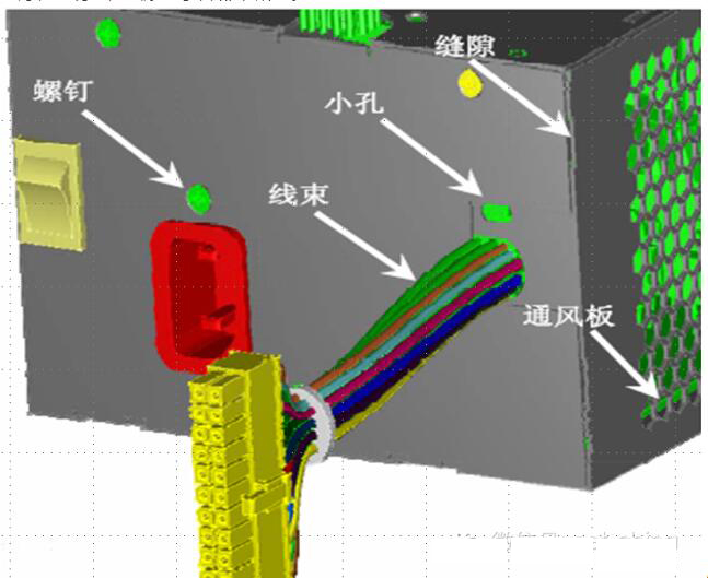
There are many actual shielding electromagnetic leakage source, for example: different parts of junction gap, vents, display window, buttons, lights, cable, power line, as shown in figure 7.
Fig. 7 electromagnetic leakage source on the actual shield
1 slot shield
When the gap is close to half the wavelength, the electromagnetic wave will leak out. This type of electromagnetic leakage source is slit antenna. When the gap size is close to half wavelength, the electromagnetic leakage is the largest. Therefore, the high frequency should be particularly good hole slot shielding, requiring a long slit or aperture is less than l/100. Electrical continuity must be maintained throughout the joint to avoid the formation of slot antennas. At least in every l/6 there is connected with the electric contact surface between the fastening points directly connected (including screw rivet lock and other welding???). Permanent joint, welding process. The joint formed by the non permanent mating surface is made of conductive gasket. It can reach 20dB/1GHz.
The continuity of the shield is the most important factor affecting the shielding effectiveness.
2 treatment of ventilation holes
The purpose is to deal with the contradiction between shielding and heat dissipation.
Waveguide is a tubular metal structure, the characteristics of high pass filter, high frequency electromagnetic wave through the waveguide, low frequency electromagnetic wave is very large loss. The waveguide in the cutoff region is called the cutoff waveguide, which can suppress the frequency of the disturbance in the cutoff region. The device is called a cut-off waveguide window, as shown in Figure 8, which is used for high shielding effectiveness. .
Fig. 8 cutoff waveguide ventilation window
The ventilation window below the cutoff waveguide can inhibit the 10GHz effect of 50-80dB/1GHz. screen harassment, but the cost is high, the waveguide aluminum paste form, subject to the conductive oxide, tin, nickel conductive treatment, the price more than 1000 yuan. /m2 steel made by soldering waveguide, the price is expensive, is not recommended to use.
Shielding effectiveness of the cabinet is not high, can be made of metal hole plate, as shown in figure 9. Only applies when the disturbance frequency is lower than 50MHz, the screen effect is 30-50dB/1GHz. Material for steel plate or aluminum plate.
Fig. 9 metal orifice plate
3 monitor: the use of metal coated conductive glass
The metal coated glass by vacuum sputtering process in general or toughened glass surface to form a dense conductive film made of, has high shielding effectiveness, the advantages of high light transmittance, no optical distortion, strong adaptability to the environment.
4 cable or wire traversing shield
Filter connector used for multiple wire or cable through the shield. Capacitor, feedthrough filter for single wire or cable through the shield.
5 continuous design
The correct connection method of shielding layer should adopt the crimping terminal and 360 degree lap to form the dumbbell shaped structure.
Fourth layer filter design
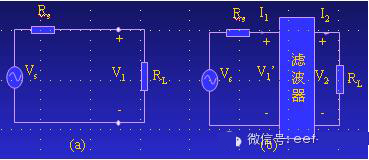
Conduction disturbance can be transmitted through the power lines, signal lines, interconnection lines and other conductors, as well as shielding, grounding conductor and other conductors. The method of solving the conduction coupling is to remove the disturbance from the conductor or conductor by filtering before the disturbance enters the sensitive circuit.
EMI filter, EMI filter, is the most effective means to suppress the conduction disturbance. The utility model comprises a signal line filter and a power line filter. The signal line filter allows the useful signal to pass without attenuation, while greatly reducing the clutter disturbance signal. Power line filter, also known as the power grid filter, it is to reduce the attenuation of DC, 50Hz, 400Hz power supply to the device, but greatly attenuated by the power of the incoming EMI signal to protect the equipment from its harm. At the same time, it can inhibit the EMI signal generated by the equipment itself, prevent it from entering the power grid, pollute the electromagnetic environment and endanger other equipment.
EMI filter, usually a lumped parameter, passive low-pass filter. But the EMI filter is different from the general low-pass filter, the EMI filter is more concerned about the insertion loss, energy attenuation, cut-off frequency and other characteristics.
A key characteristic of the filter performance
1 one of the key characteristics that affect the performance of the filter
The passive filter is composed of an inhibitory component, which depends not only on the component parameters, but also on the termination impedance. As shown in figure 10.
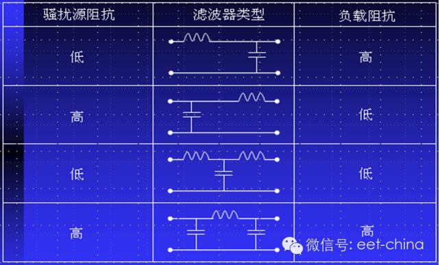
Figure 10 source / load impedance and filter network structure selection
For example, in order to prevent the instability of the power system, the output impedance of the filter must be less than the input impedance of the switching power supply. The input impedance of the filter should be different from the output impedance. Its purpose is to make it possible to match as much as possible in order to obtain the maximum insertion loss.
2 the key characteristics of the filter performance of the two: frequency characteristics
EMI filter noise suppression capability evaluation index: insertion loss IL (Insertion Loss). The definition of insertion loss is shown in figure 11.
圖11 插入損耗的定
.jpg)
Common mode and differential mode insertion loss is measured in the system of a resistance 50~75W between in the optimization and is misleading, 100/0.1 or 0.1/100 system can truly practical application of the performance prediction.
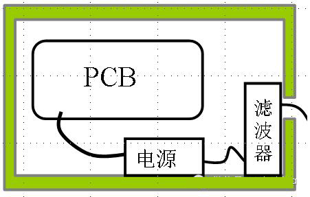
3 the key characteristics of the filter performance of the three: power line filter installation
When the power line filter is installed, it is easy to appear, including the long input line, the coupling between the input and output, the bad grounding and so on. To solve these problems, the correct installation of the power line filter should be shown in figure 12.
Fig. 12 correct installation of power line filter
Fifth layer transient disturbance rejection design
Suppression of electrical fast transient pulse group (EFT)
Inhibition of EFT should be done: the selection and installation of power filter and signal filter is correct: reducing PCB loop area and lead inductance; classification of binding wire and cable laying classification; shielding line line, power line should not be too long; the right to install grounding design; transient disturbance suppression.
Two. The suppression of lightning surge
The failure of the lightning surge test results in the high differential mode voltage leading to the breakdown of the input device, or the high common mode voltage leading to the breakdown of the insulation between the line and the ground.
Measures to be taken by lightning surge sensitivity test: surge absorber should be used at the entrance of the inlet line. A signal line and a power supply line may not be passed near the device to prevent the introduction of surge into the signal and power supply lines. The pin of the device should be short; the absorption capacity should match the test level of surge voltage and current.
Three. Electrostatic protection
Electrostatic discharge is large current transient high voltage, strong electric field. The fast rise time, short duration (the majority of only a few hundred nanoseconds) electromagnetic pulse.
1.ESD protection is a system engineering, all aspects need to implement comprehensive control. The general protection of 2000V (+ / -) should meet the above requirements.
Design of ESD protection circuit for 2.. Electronic equipment
The release of the bypass protection circuit: its role is to charge through the protection circuit to release, to avoid damage to the function of electrostatic components; limited voltage / current limiting protection circuit: its role is to slow down the electrostatic discharge, the discharge voltage / current small, clamp device port; the insulating medium such as plastic chassis, the air gap and the insulation material of the internal components and systems from outside;. Use a metal shielding shell, to prevent the internal circuit of the ESD current impact; optical coupler, isolation transformer, optical fiber / wireless and infrared coupling installed on the.PCB board, to achieve electrical isolation.
Four. Transient suppressor
Because the input and output impedance of filter and power grid and the load impedance of a serious mismatch, very limited ability to suppress the transient disturbance. The most effective way is to use transient suppressors, most of the energy transfer to the ground.
1 lightning tube: early lightning arrester tube is a gas discharge tube, an electrode may be coupled transient disturbance line, another ground. The transient disturbance occurs, the tube gas is ionized, the voltage between the two poles quickly dropped to a very low value of residual pressure (2-4kV), the most transient energy is ground rapidly, large current capacity (more than 100kA), power consumption is greatly reduced, low leakage current, the product is protected. Has been cured, small size. Lightning surge current tube has strong absorption ability, high insulation resistance (>104MW) and parasitic capacitance is very small (<2pF), the product will not have a detrimental effect on the normal work. But time is slow, the response is about? 100ns. is only applicable to a product line protection and protection.
2 varistors (VSR) (varistor; voltage-dependent resistor): for a plurality of PN junction together in parallel and series voltage sensitive clamp protection device. When the voltage across the ends of the varistor below the nominal voltage, the resistance is nearly infinite, while more than nominal varistor voltage value, the resistance will drop rapidly. It absorbs the effect on transient voltage is achieved by clamping mode, and converted into heat. The main parameters of the response time for <50ns:
1) nominal varistor voltage V1mA, the breakdown voltage or threshold voltage. Refers to the provisions of 1mA voltage and current values under 1mA DC when the measured voltage value is 109000V ranging. General V1mA=1.5Vp or V1mA=2.2VAC, in the formula, Vp is the peak of the rated voltage of the circuit. VAC is the RMS value of the rated AC voltage. The selection of voltage value of ZnO varistor is very important, it relates to the protection effect and service life. If the rated supply voltage is 220V, then the breakdown voltage of V1mA=1.5Vp=1.5 * 1.414 * 220V=467V, V1mA=2.2VAC=2.2 * 220V=484V. or so, in between 470480V.
2, the current capacity (kA), that is, in the ambient temperature of 25 DEG C, the peak of the maximum pulse current, usually choose from 2 - 20kA.
3, residual voltage ratio: the peak value of 8/20ms standard impulse current through the varistor, the peak value of both ends of the voltage (called the maximum limit voltage) and the ratio of the varistor voltage. About 1.7-1.8.
3.TVS (Transient Voltage Suppresser transient voltage suppressor)
With the rapid development of electronic information technology, semiconductor devices are becoming more and more miniaturization, high density and multifunction. So the protection devices must have low clamping voltage ESD to provide effective protection; and faster response time to meet the requirements of high speed data lines; high integration package for printed circuit board of portable equipment shortage; and also to ensure many times after the ESD process will not deteriorate to ensure high quality of equipment. TVS (Transient Voltage Suppresser transient voltage suppressor) is generated in order to solve these problems, it has become the key technology of electronic information equipment protection device, is specially designed for solid element absorption of ESD energy and protect the system from being ESD damage.
TVS is a diode form of high efficiency protection device. When the TVS diode poles by the reverse transient high energy impact, it can take 10-12 seconds of the speed, the high impedance between two poles into low impedance, absorb up to several kilowatts of power surge, the voltage clamp between two poles at a predetermined value, the effective protection of electronic circuit in precision components the damage from the surge pulse. Because of its fast response time, transient power, low leakage current, breakdown voltage of small deviation, the clamp voltage is easy to control, no damage limit, small volume etc..
It has been widely used in computer systems, communication equipment, AC / DC power supply, automobile, electronic ballasts, household appliances, instruments, RS232/422/423/485, I/O (meter), LAN, ISDN, ADSL, USB, MP3, PDAS, GPS, CDMA, GSM, digital camera protection, differential protection, / common mode RF /IC drive coupling fields receiving protection, electromagnetic disturbance suppression, audio / video input sensor, motor / gearbox, control circuit, relay and contactor noise suppression.
Sixth layer system level EMC design
The influence of EMC on system performance include: system performance degradation or failure; reduce the system reliability; system working life; influence effect / cost trade-off; affect the survival and security system and personnel; the production and use of delay. System level EMC design flow shown in figure 13.
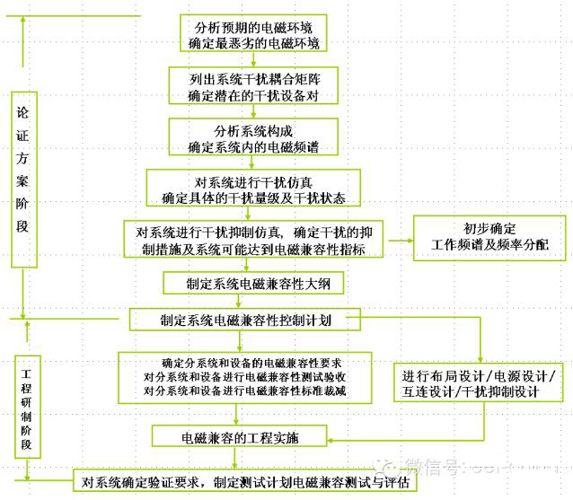
Figure 13 system level EMC design flow
The practice shows that the EMC+EMC / EMC system can not guarantee the EMC of the system, which satisfies the limitation of equipment EMC. It is therefore important to specify the EMC requirements of the system and to implement it in the same way as to ensure that the device EMC is. For example, if the values of the field strength measured by the N modules are equal to each other, the
Eo=N1/2E (mV/m)
Set the standard limits for the harassment of the launch of Eo, if there are N modules, each module should be the limit of the disturbance emission
E=Eo/N1/2
More than ten years, "electromagnetic compatibility layer and integrated design method has been successfully used for EMC design of synthetic aperture radar satellites, large container inspection system, handheld machine, integrated circuit, automotive electronic system, medical electronic equipment and systems, such as embedded robot controller, basic achieve EMC test a success.


.jpg)
.jpg)


 銷售客服
銷售客服